In the previous post, we had a look at designing a general purpose board based on the popular AT89S51 MCU. We took advantage of the fact that the S variant of Atmel's 8051 series allows ISP(In-System programming) and hence we used an Arduino as the in-system programmer to burn code onto our board by means of the protocol SPI (Serial Peripheral Interface). In this post, I would like to detail what SPI is, how can one design it in HDL(Hardware descriptive language) and upload our SPI module onto an FPGA and use that to program our 8051 board.
Brief Review of Intel HEX format
If you followed the previous 8051 tutorial, you'll remeber that we burned in a sample blinky.hex program onto our 8051 board to make it blink with an approximate delay of 1 second. The contents of the assembly file are as given below
ORG 0000H
        SJMP BLINKY

DELAY:  MOV R0, #08H            ;Delay of 1 Machine Cycle
DELAY2: MOV R1, #0FFH           ;Delay of 1 Machine Cycle
DELAY3: MOV R2, #0FFH           ;Delay of 1 Machine Cycle
AGAIN:  DJNZ R2, AGAIN          ;Delay of 2 Machine Cycle
        DJNZ R1, DELAY3         ;Delay of 2 Machine Cycle
        DJNZ R0, DELAY2         ;Delay of 2 Machine Cycle
        RET                     ;Delay of 2 Machine Cycle

BLINKY: ACALL DELAY             ;Delay of 2 Machine Cycle
        CPL P1.4                ;Delay of 1 Machine Cycle
        SJMP BLINKY             ;Delay of 2 Machine Cycle


END
I have commented the delay in number of machine cycles so that the reader can confirm that the blink period is indeed 1 second (you need to factor in the crystal frequency of 24 MHz which results in each Machine cycle being 0.5u seconds).
The mneumonics representing the instructions such as SJMP are in reality a HEX code/number. The assembler is responsible for translating an assembly program containing mneumonics to machine language file containing purely HEX codes. The HEX file contents can be understood by replacing our assembly language file mneumonic instruction line by line with the corresponding HEX code.
ORG 0000H                       ;    Address    HEX code    Reasoning
        SJMP BLINKY             ;    0000H      800DH       80 represents SJMP and 0D is address of BLINKY(000FH) relative to PC(0002H)

DELAY:  MOV R0, #08H            ;    0002H      7808H       78 represents MOV R0 and 08 is the immediate operand 08H
DELAY2: MOV R1, #0FFH           ;    0004H      79FFH       79 represents MOV R1 and FF is the immidiate operand FFH
DELAY3: MOV R2, #0FFH           ;    0006H      7AFFH       7A represents MOV R1 and FF is the immidiate operand FFH
AGAIN:  DJNZ R2, AGAIN          ;    0008H      DAFEH       DA represents DJNZ R2 and FE is the address of AGAIN(0008H) relative to PC(000AH)
        DJNZ R1, DELAY3         ;    000AH      D9FAH       D9 represents DJNZ R1 and FA is the address of DELAY3(0006H) relative to PC(000CH)
        DJNZ R0, DELAY2         ;    000CH      D8F6H       D8 represents DJNZ R0 and F6 is the address of DELAY2(0004H) relative to PC(000EH)
        RET                     ;      0EH        22H       PC is loaded with SP(0011H)

BLINKY: ACALL DELAY             ;    000FH      1102H       11 represents ACALL and 02 represents the address of DELAY(0002H), SP is loaded with PC(0011H)
        CPL P1.4                ;    0011H      B294H       B2 represents CPL and 94 the address of Port 1 bit 5
        SJMP BLINKY             ;    0013H      80FAH       80 represents SJMP and FA represents the address of BLINKY(000FH) relative to PC(0015H)


END
The HEX file for the above program is as given below
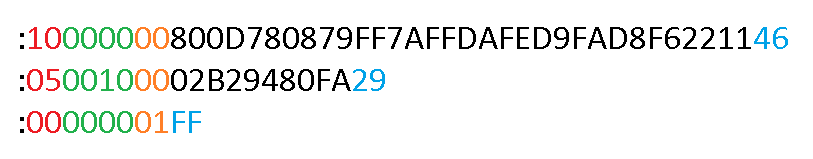
I have marked the nibbles according to what they represent
-
Red nibbles represent the number of data bytes (black nibbles) in that line.
-
Green nibbles represent a 2 byte address which indicates where that particular line is going to be written in the PROM of 8051
-
Black nibbles represent the data. If you notice carefully, this matches the HEX code we wrote down
-
Orange nibbles represent whether that particular line has data bytes or if its end of file. 00 = data bytes and 01 = end of file
-
Blue nibbles represent the checksum for that line which is used to ensure integrity of the code burnt in
Serial Peripheral Interface (SPI)
Now that we have seen the HEX file for our assembly program, it is this HEX file we are going to transfer to our 8051 byte by byte using SPI. SPI is a full duplex (simultaneous transmit and receive) synchronous communication protocol. The signals required for SPI to work are
- SCK (Serial Clock)
- MISO (Master In Slave Out)
- MOSI (Master Out Slave In)
- SS (Slave Select)
SPI can have more than one slave but only one master.
SCK
-
The master is responsible for generating the serial clock. The maximum frequency/baud rate is dictated by both the master and slave's receive rate. For 8051, the max baud rate allowed is $\frac{1}{16}$th of crystal frequency. Since our crystal frequency is 24Mhz, the max baud rate is 1.5MHz. The SCK is used to synchronize data transfers and initiate state changes in our FSM based SPI module.
MISO
-
MISO is the line on which the slave transmits data and the master receives data.
MOSI
-
MOSI is the line on which the master transmits data and the slave receives data.
SS
-
Since SPI can have more than one slave, the SS is used to select a particular slave for communication. Since we are interested in using SPI for burning programs, we will be dealing with a single slave and hence this signal is not relevant for us.
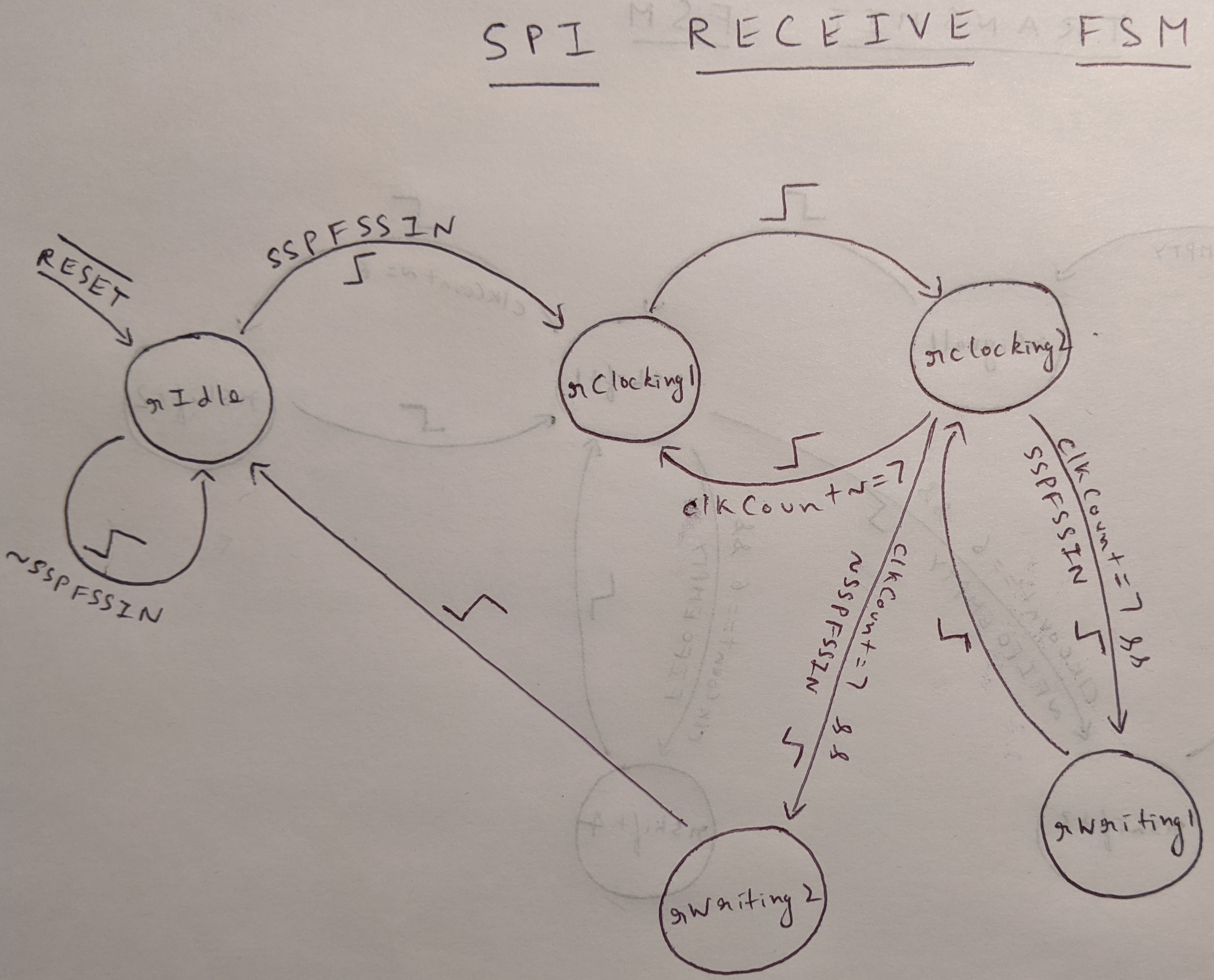
The transmit FSM
![]()
and the receive FSM
The behavioural simulation of the verilog module is as follows
![]()
- SSPTXD is our MOSI
- SSPCLKOUT is our SCK
- PSEL is our SS
Since PCLK is faster than SSPCLKOUT, I have added a FIFO buffer in the transmit module to prevent data loss. The FIFO buffer depth can be varied. The SSPTXINTR signal indicates that the FIFO buffer is full and hence anymore data sent to the transmit module to be written will be lost. PWDATA is the data to be written/sent whereas CLEAR_B is our reset signal.