Found some time to work on hobby projects for thanksgiving break and seeing that I had to limit myself to using IC packages with extended leads due to lack of a way to soldering them, I decided on building a Solder Reflow Oven 2.0 !
The first version was built around an AT90USB646, it worked fine but it used a separate 12V dc adapter to power the board. This time around I wanted to power the board and the reflow oven from the mains and also add some TFT LCD tech to make it more rad!! This version uses an STM32L053 mcu based on ARM Cortex M0+. Well, thats all the motivation/excuse I needed to build Solder Reflow Oven 2.0
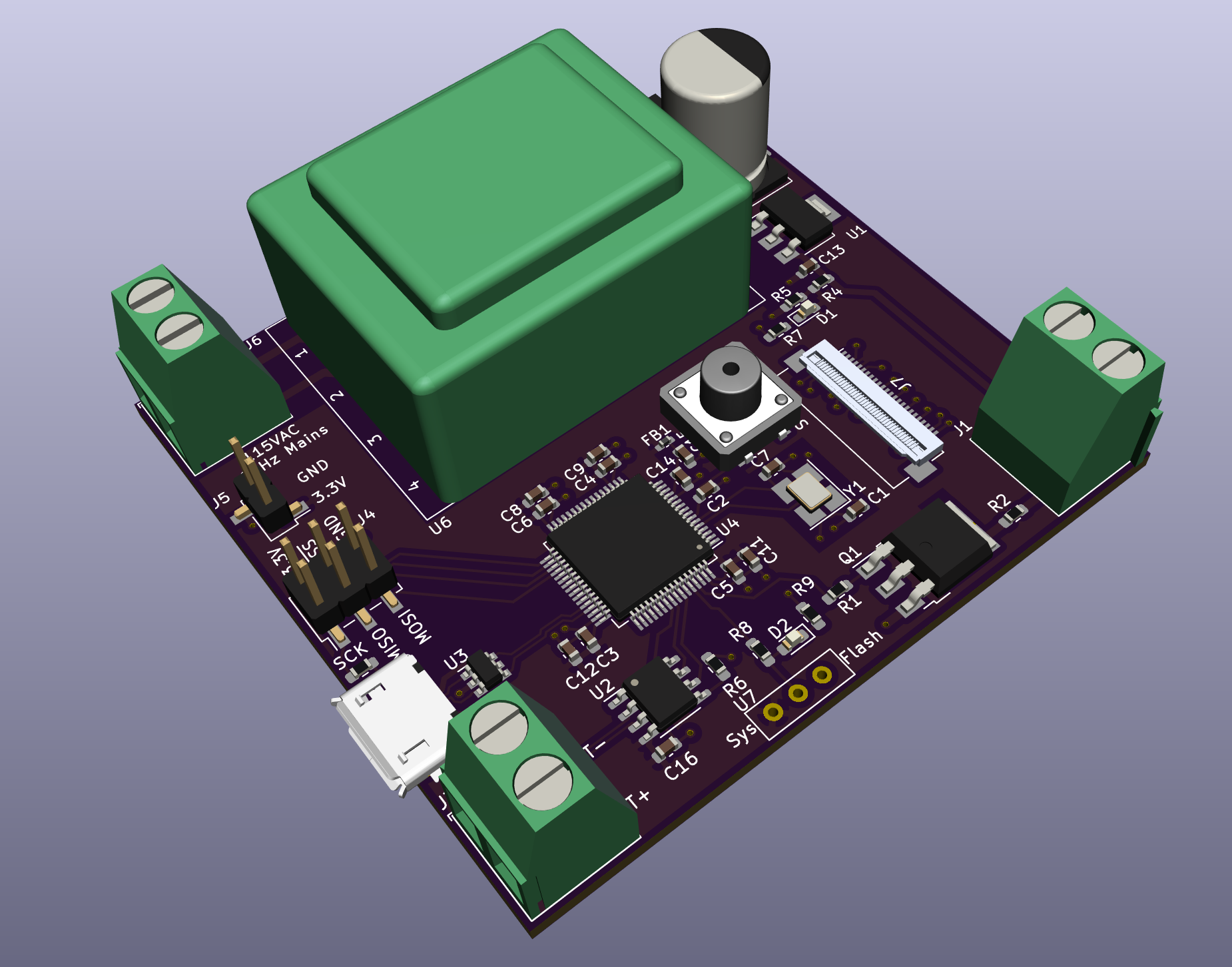 Figure 1 : 3D model of the Solder Reflow Oven Controller
Table of Contents
Power Supply
I did not want to deal with multiple wires coming in and out of the oven so I decided to power the board from the mains. This meant incorporating an AC to DC (3.3V) stage. The stage consists of a rectifier implemented using a diode-bridge, before rectifying I step down the voltage from 115V to 24V so that I can use components (diodes, capacitors) rated at lower voltages which makes the entire build cheaper.
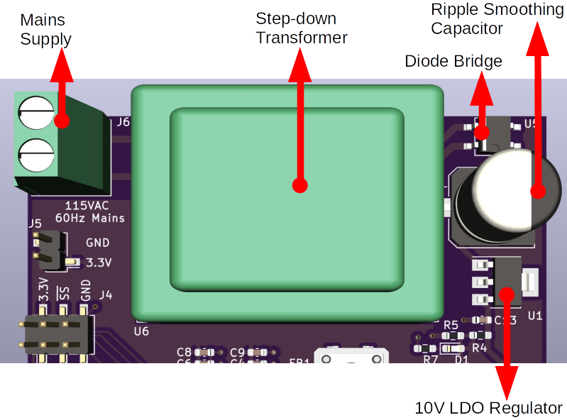 Figure 2 : 3D model of the power stage
On applying the stepped down AC to the diode bridge, we obtain a pulsating DC at the output. To smooth this pulsating DC we can use a large capacitor. Once the capacitor fully charges to peak value of the pulsating DC, it can practically supply charge with minimal drop in its voltage till it charges again. This helps remove ripple and produce a constant DC voltage. The output of the ripple smoothing capacitor is then input to a 10V regulator to obtain a 10V stable output.
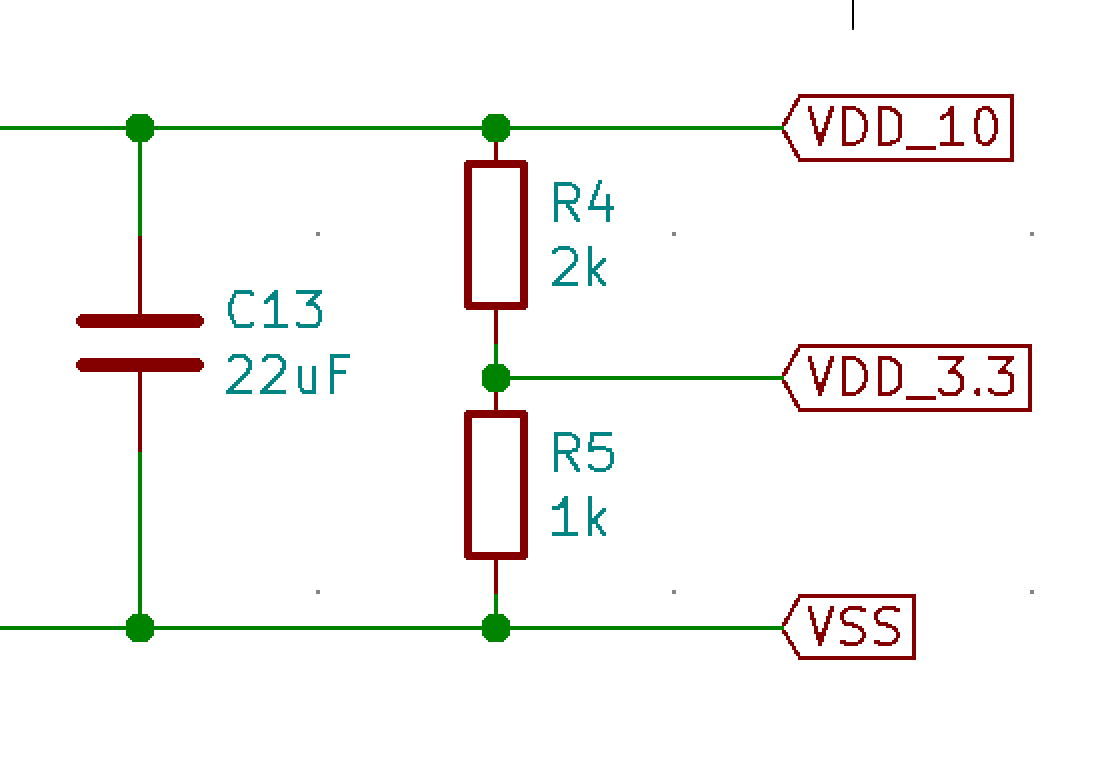 Figure 3 : Schematic of 10V and 3.3V supply generation
I then use a R2R divider to obtain 3.3V from the 10V rectifier output. Although this is not the most efficient way to do it, this isn't much of a problem at low voltages or power. We would have needed a buck converter if the power involved was higher to improve efficiency of the conversion from 10V to 3.3V.
Crystal Layout
The crystal oscilator unit perhaps contains the highest frequency signals (24MHz) in our board. For this reason we must take care in routing and placing it in such a way that it doesn't couple onto nearby traces nor it get affected due to noise in nearby traces. Capacitive and inductive coupling are inevitable when traces are routed in close proximity to each other, however, we can decrease the extent of such coupling by following certain guidelines during route and placing. Capacitive coupling primarily depends on :
- Overlap area - long sections of parallel traces increases capacitive coupling (more noise)
- Distance to ground plane - large distance between signal and ground plane increases capacitive coupling (more noise)
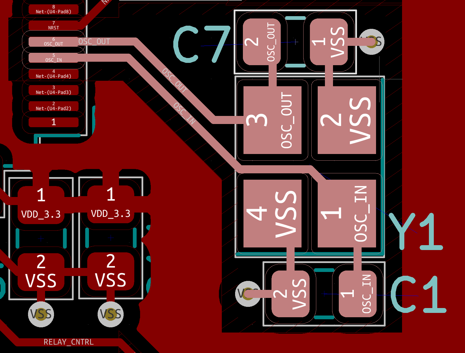 Figure 4 : Crystal layout on top Cu layer
In the above layout, the highlighted components and traces correspond to the crystal unit. By restricting other signal traces and copper pour around my crystal unit I can reduce the overlap area (see above points) and thereby reduce capacitive coupling. Distance to ground plane is reduced by opting for a 4-layer board but I think this layout should be sufficient for the frequencies I am working at and should work without any issues with a 2-layer board.
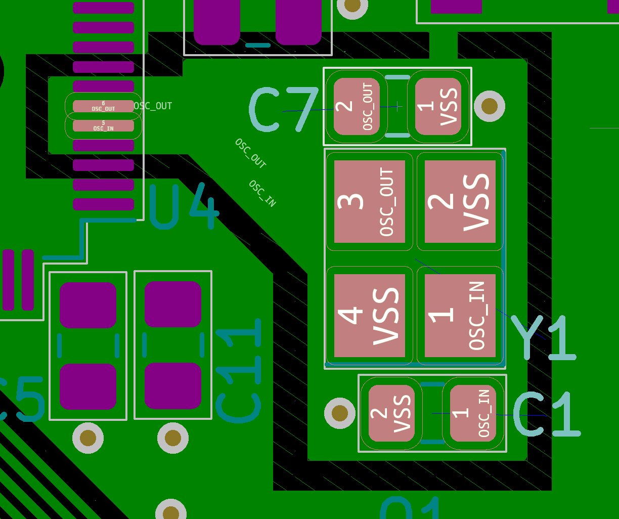 Figure 5 : Crystal layout on bottom Cu layer
I also use a local ground plane for the crystal unit and tie it to the global ground at a single point. This prevents any other high frequency return currents from flowing under the crystal unit (this is due to increase in inductance due to larger loop area that these return currents would have to take if they flowed under the crystal unit's local ground). This further improves the integrity of all signals involved in our crystal unit.
Controlling the Relay
The relay I used requires about 15mA of current to turn on, the STM32L053 can deliver it but while operating at near its max rating which decreases its lifetime. Instead, I use an NPN bjt to drive the relay while controlling it with the mcu.
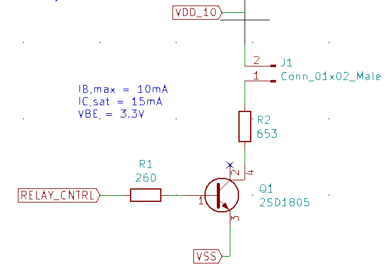 Figure 6 : NPN BJT biasing schematic
I bias the NPN such that it operates in either cut-off or saturation. Cut-off is easy, we just make Vbe 0. To drive it into saturation we need to ensure that Vce is driven into saturation, from the datasheet for 2SD1805 we see that the typical value for Vce,sat is 0.22V. Therefore, we need to choose Rc such that Vce is Vce,sat when Ic is 15mA. Hence, Rc = (10-Vce,sat)/Ic = (10-0.22)/0.015 = 652 Ohms. I use 653 Ohms for Rc. Since Ic is independent of beta in saturation, we can choose Ib independent of Ic as long as its sufficient to make Vbe > 0.7V (turn on base-emitter junction). I chose Ib to be 10mA from which I calculate Rb = (3.3V - Vbe)/Ib = (3.3 - 0.7)/0.01 = 260 Ohms. I therefore, use 260 Ohms for Rb.
Testing the Circuit
Finished my finals this week, so I found some time to test the board. I first did continuity tests with a multimeter before powering the board to make sure there aren't any shorts (especially between the voltage rails). To test the board, I powered it with a variac (variable output transformer) for safety reasons. The measurements I took are given below
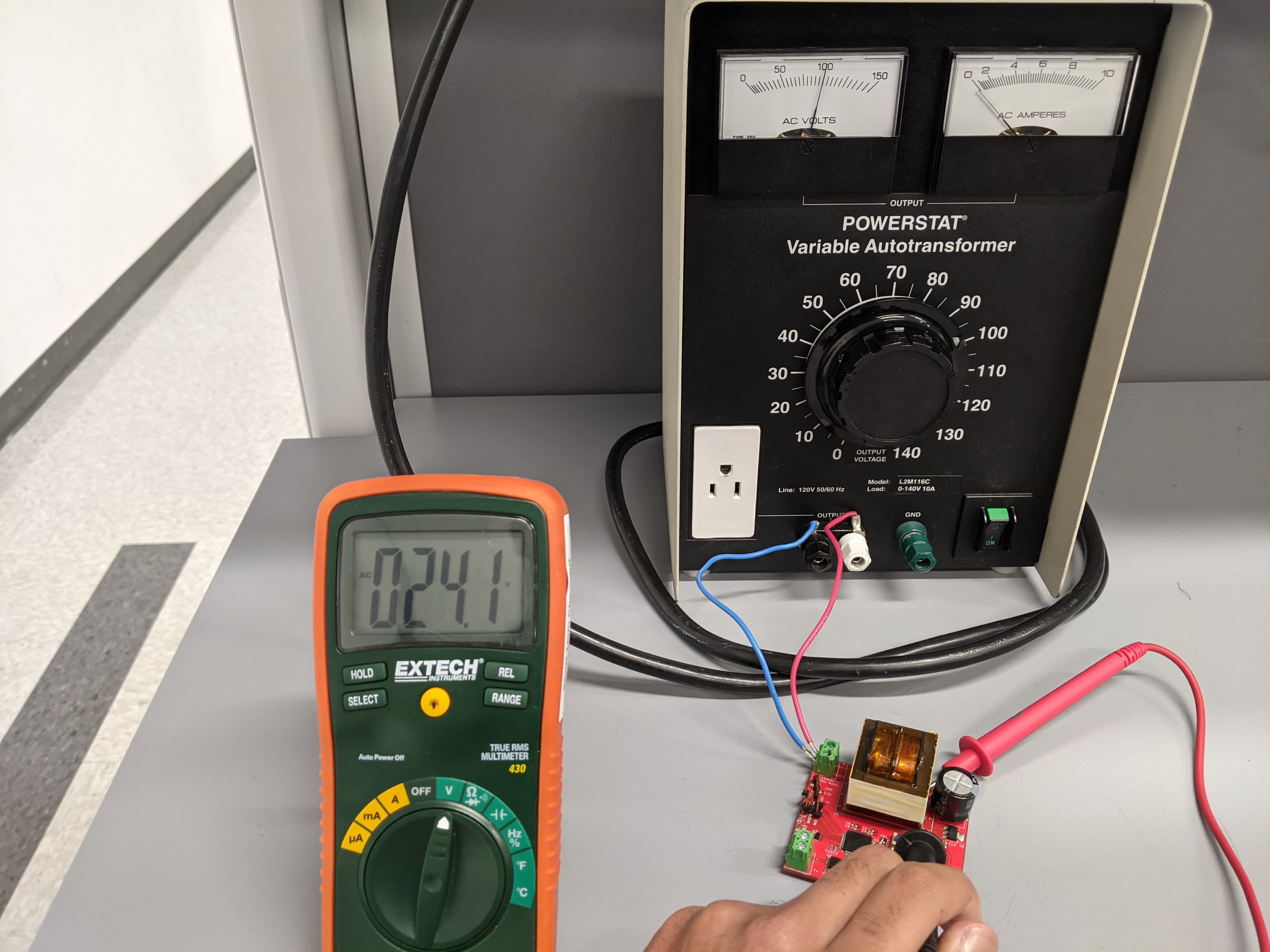 Figure 7 : RMS voltage measured at the secondary of the transformer
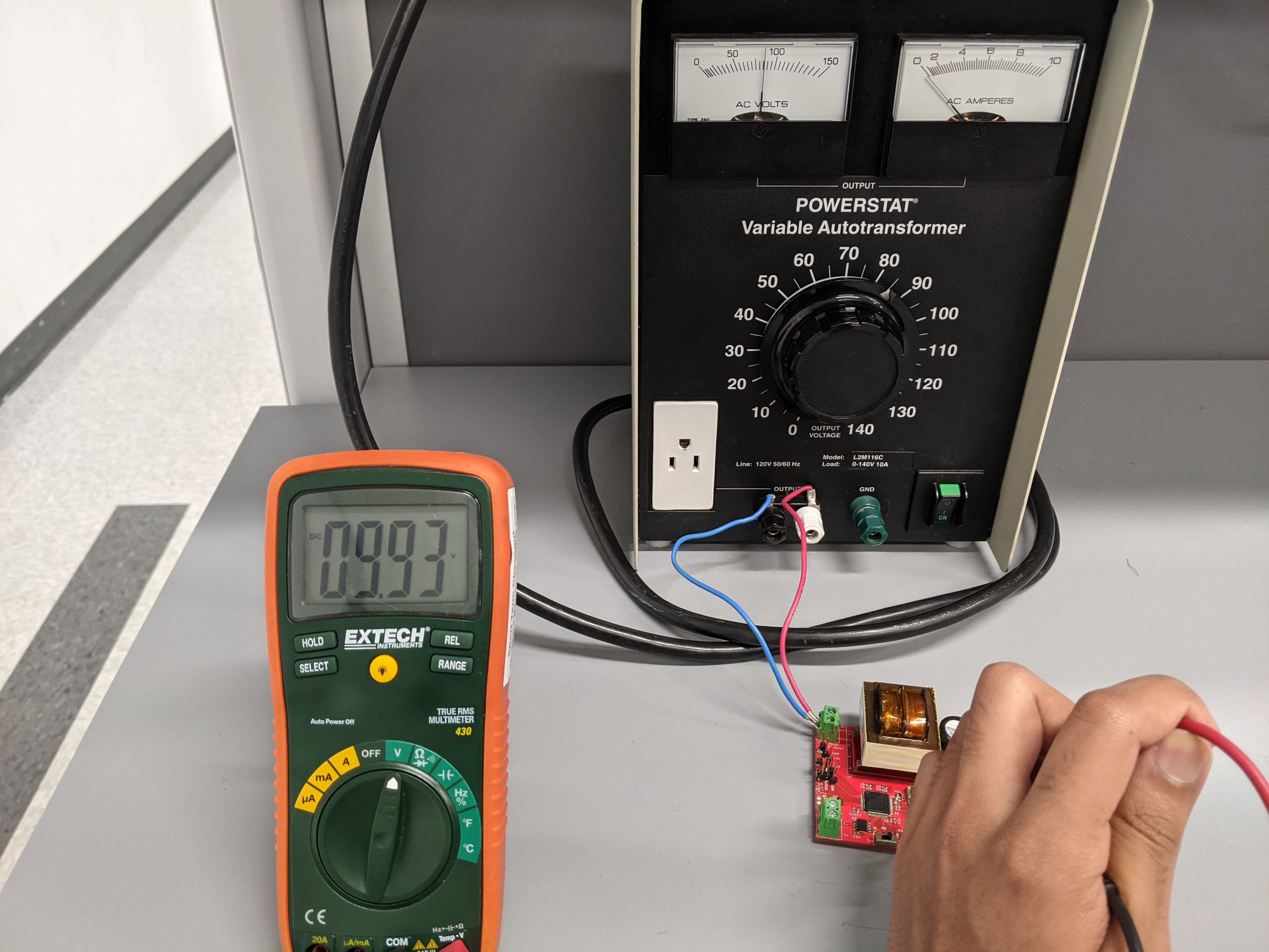 Figure 8 : DC voltage measured at the ouput of the 10V regulator
I made two mistakes (they can be corrected on the board itself but I learnt a great deal from them). In the Fig.7, I am measuring the AC voltage across the secondary of the step-down transformer and in Fig.8 I am measuring the DC voltage at the output of the regulator (LM2940IMPX-10). Explanation of each of the measurements warrants a subsection of its own, so lets get started
Transformer Secondary Voltage
This is where I made my first mistake. You can see from the Fig.7, the secondary voltage is 24V RMS for an input of ~100V RMS. The datasheet for F24-100-C2 said to expect 24V RMS for 115V RMS input, so clearly there's a deviation but the mistake I made is interpreting these voltages as peak rather than RMS. As stated before, the ripple smoothing capacitor(470uF) charges to the peak input of pulsating DC. According to my calculations it would've charged to 24V but since this is RMS, in reality it charges to 24xsqrt(2)=~34V which exceeds the input range of the 10V regulator I am using (LM2940IMPX-10). So this circuit will clearly not work if I powered it directly from the mains.
But luckily, there is a simple work around. Take a look at the step-down transformer layout on the board below
![]() Figure 9 : Layout of the step-down transformer
Figure 9 : Layout of the step-down transformer
It is a dual secondary transformer, there is a center tap at pins 6 or 7 at which the voltage is half (12V RMS) of the total output voltage (24V RMS). By simply
soldering pad 8 to pad 6 and clipping the transformer pin corressponding to pad 8 we can ensure that the ripple smoothing capacitor charges to only 17V RMS
which is well within the operating ranging of the regulator (6-26V).
Regulator Output Voltage
As we saw before, I was able to get a 10V DC at the ouput of the regulator when I ensured that the transformer output was below 26V peak (~19V RMS). So I know that that portion is working perfectly fine, however, when I measured the voltage at any 3.3V pins, I got a near 0V DC reading. So clearly, there is still something wrong with the board and this where things get exciting. Spoiler : It has to do with the way I am generating 3.3V from 10V , specifically resistors R4 and R5 as shown in Fig.3. Fret not! once again, the fix is easy but the learning is immense and worth it.
In Fig.3 I am using a voltage divider to generate the 3.3V supply from the 10V supply, this circuit would work perfectly fine in isolation. However, when we connect a load in parallel with R5, the voltage drop across R5 now depends on the effective parallel impedance and not just the resistance of R5. Voila, our port VDD_3.3 is no longer guaranteed to be at 3.3V.
Lets take a look for two loads 10 KOhms and 100 Ohms. With 10 KOhms in parallel with R5, since R5 is much smaller than 10 KOhms, the effective parallel impedance is closer to R5 and is 900 Ohms. Therefore, the voltage at port VDD_3.3 is now 3.1V instead of 3.3V but is still close enough to not significantly impact the working of any components on board. Now lets connect 100 Ohms, the effective parallel impedance is now 90 Ohms and so the voltage at port VDD_3.3 is just 0.4V !! Much lower than the expected 3.3V and will obviously cause almost all components to stop working.
For a closer analysis, and to demonstrate the above scenario, I performed a DC-IR drop analysis. To do so I converted the KiCAD project into Altium and exported it as a ODB++ file. I imported this into Ansys SIWave and assigned the components their appropriate values. I then assigned a voltage source of 10V to the output of the regulator (U1 LM2940IMPX-10) and current sinks across VDD and VSS pins of the STM32L053 (20mA from datasheet) and MAX31855(1.5mA from datasheet). The results of the DC-IR drop analysis for two pairs of R4 and R5 values are shown below
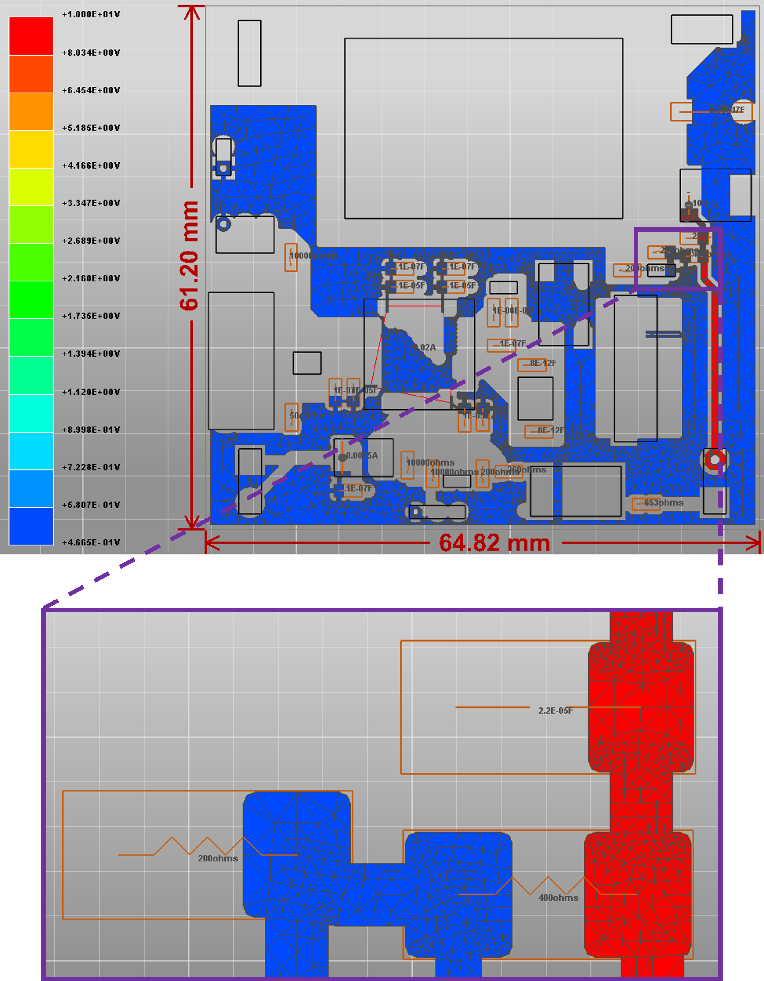 Figure 10 : DC-IR drop analysis with R4 = 400 Ohms and R5 = 200 Ohms
In Fig.10, I have set R4 and R5 as 400 Ohms and 200 Ohms respectively. This demonstrates the condition where the load impedance in parallel with R5 is much smaller than R5. We see that the 10V net (in red) is as expected at 10V, however the power plane corressponding to 3.3V is at just ~0.46V !! This implies that almost all of the 10V is dropped across R4.
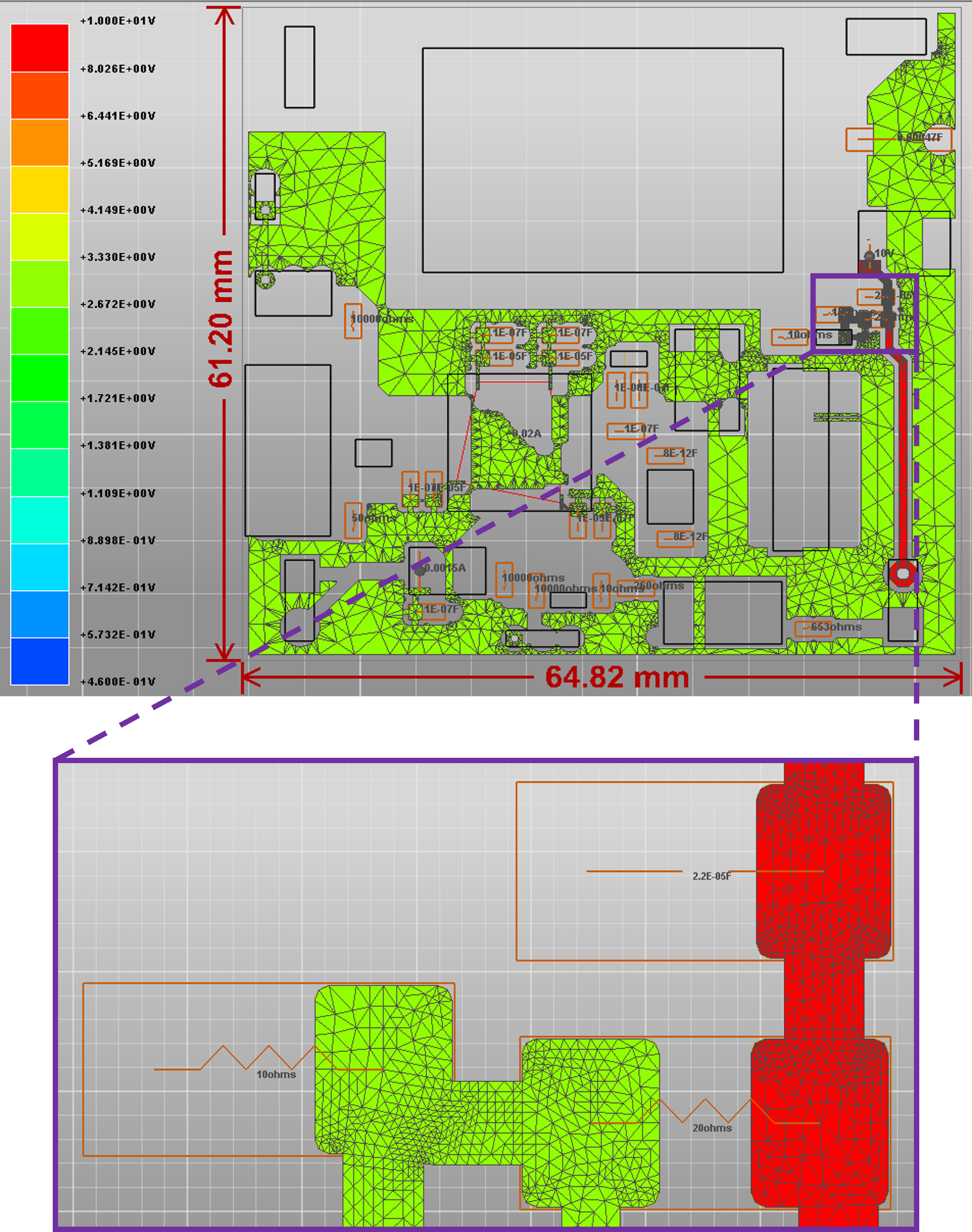 Figure 11 : DC-IR drop analysis with R4 = 20 Ohms and R5 = 10 Ohms
In Fig.11, I have set R4 and R5 as 20 Ohms and 10 Ohms respectively. This demonstrates the condition where the load impedance in parallel with R5 is much larger than R5. We see that once agains the 10V net (in red) is as expected at 10V and this time the power plane corressponding to 3.3V is at ~3.2V as required.
So to rectify my board, I have to replace R4 and R5 with smaller values while keeping their resistance ratio 2:1. Nevertheless, this is not a good way of designing the power supply for the 3.3V power plane (I'll discuss a better way). The reason is because, although choosing a smaller R4 and R5 fixes the issue with voltage drop, a larger current is going to be sunk by R5 regardless of the current demands of other components connected to the 3.3V power plane. This is shown in Fig.12.
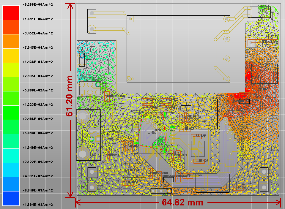 Figure 12 : Surface Current distribution with R4 = 20 Ohms and R = 10 Ohms
Better Alternative for powering 3.3V Power Plane
We see that just using smaller values for R4 and R5 is a terribly inefficient way to power the 3.3V power plane due to the current comsumption being extremely high regardless of the demands of the on board components. The easiest and better alternative is to use a buck converter to buck the 10V to 3.3V. Another way is to use a voltage divider in conjuction with an opamp configured as a voltage follower as shown in Fig.13.
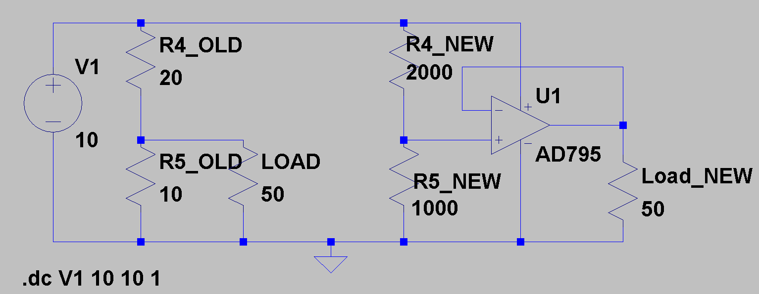 Figure 13 : SPICE DC simulation of two variations of Voltage Divider
Fig.13 contains two variations of the voltage divider. To the left we see the voltage divider we have discussed so far, to ensure that the voltage drop across R5_OLD is close to 3.3V we have to ensure that R5_OLD is smaller than LOAD (50 Ohms) but this implies a larger current sunk by R5_OLD. So ideally, we want to use large values for R4 and R5 since this decreases the current sunk by R5 thus improving the efficieny of the circuit but then the voltage drop across R5 is extremely small due to the LOAD being smaller than R5. We can overcome this by using a voltage follower as shown in the right half of the circuit in Fig.13. Since an opamp configured as voltage-follower has ideally infinite input impedance this implies that we can use large values for R4 and R5 as shown by R4_NEW and R5_NEW without compromising on the 3.3V drop across R5_NEW on connecting the LOAD. The opamp as a voltage-follower acts as a buffer, isolating the output and input. The current through R5_OLD is 0.3A whereas that through R5_NEW is 3mA, about 2 orders of magnitude lower. The voltage drop across R5_OLD is 2.9V and that across R5_NEW is 3.3V and therefore the voltage divider version on the right of Fig.13 not only provides a consistent 3.3V output regardless of the load connected to it but by using large R4 and R5 we can also improve the efficiency of the circuit.
Update and Modified Design
Bill of Materials
| Component | Quantity | Total Cost | Description |
|---|---|---|---|
| 511-STM32L053R6T6 | 1 | $5.32 | ARM Microcontrollers - MCU ARM Microcontrollers - MCU 16/32-BITS MICROS |
| 947-RCLAMP0502A.TCT | 2 | $1.82 | ESD Suppressors / TVS Diodes ESD Suppressors / TVS Diodes Low Capacitance TVS Array, 5V |
| 863-2SD1805F-TL-E | 3 | $2.91 | Bipolar Transistors - BJT Bipolar Transistors - BJT BIP NPN 5A 20V |
| 700-MAX31855KASA+T | 1 | $5.38 | Sensor Interface Sensor Interface Cold-Junction Compensated Thermocouple-to-Digital Converter |
| 750-CDBHD140L-G | 2 | $3.30 | Bridge Rectifiers Bridge Rectifiers LOW VF 1A 40V Schottky Bridge |
| 621-AZ1117R-3.3TRE1 | 2 | $1.10 | LDO Voltage Regulators LDO Voltage Regulators LDO BJT HiCurr |
| 649-67996-400HLF | 50 | $1.70 | Headers & Wire Housings Headers & Wire Housings .100CC STR HEADER |
| 612-LL3301NF065QG | 2 | $1.20 | Pushbutton Switches Pushbutton Switches 50mA 12VDC F065 4.3mm Gull Wing |
| 640-FFC2B28-24-G | 3 | $1.98 | FFC & FPC Connectors FFC & FPC Connectors 24W,0.5mm FFC Con,R/A,Dual Cont,B/Flp,H1.0mm,Gld,SMT,T&R |
| 710-150060VS75000 | 20 | $2.80 | Standard LEDs - SMD Standard LEDs - SMD WL-SMCW SMDMono TpVw Waterclr 0603 BrtGrn |
| 81-GRM0335C1H180FA1D | 5 | $0.50 | Multilayer Ceramic Capacitors MLCC - SMD/SMT Multilayer Ceramic Capacitors MLCC - SMD/SMT |
| 603-CC0402KPX58BB104 | 10 | $0.43 | Multilayer Ceramic Capacitors MLCC - SMD/SMT Multilayer Ceramic Capacitors MLCC - SMD/SMT 25V 0.1uF X5R 0402 10% |
| 963-EMK107BJ105KAHT | 10 | $0.37 | Multilayer Ceramic Capacitors MLCC - SMD/SMT Multilayer Ceramic Capacitors MLCC - SMD/SMT 0603 16VDC 1uF 10% X5R AEC-Q200 |
| 963-UMK325ABJ106MMHT | 10 | $5.09 | Multilayer Ceramic Capacitors MLCC - SMD/SMT Multilayer Ceramic Capacitors MLCC - SMD/SMT 1210 50VDC 10uF 20% X5R AEC-Q200 |
| 660-RN731JTTD6570D25 | 2 | $0.62 | Thin Film Resistors - SMD Thin Film Resistors - SMD 0603 657 Ohms 0.5% 25PPM |
| 279-CPF-A-0603B1K0E | 4 | $2.04 | Thin Film Resistors - SMD Thin Film Resistors - SMD CPF A 0603 1K0 0.1% 25PPM 5K RL |
| 815-ABM824MHZD1GT | 2 | $1.24 | Crystals Crystals CRYSTAL 24.0000MHZ 18PF SMD |
| 810-MMZ1005S601HTD25 | 10 | $0.83 | Ferrite Beads Ferrite Beads 600ohm 25% 440mA |
| 474-SEN-13715 | 1 | $5.00 | SparkFun Accessories SparkFun Accessories Thermocouple Type-K - Stainless Steel |
| 553-F24-100-C2 | 1 | $5.16 | Power Transformers Power Transformers POWER XFMR 24 Vct @ 100 mA UL/cUL - Class 2/3, 115V SPLIT PACK PCB MOUNT / F24-100-C2 |
| 661-EMHS500GRA471MKG | 2 | $3.30 | Aluminum Electrolytic Capacitors - SMD Aluminum Electrolytic Capacitors - SMD 470uF 20% 50V AEC-Q200 |
| 926-LM2940IMPX10NOPB | 4 | $7.96 | LDO Voltage Regulators LDO Voltage Regulators 1-A, 26-V, high-PSRR, low-dropout voltage regulator 4-SOT-223 -40 to 85 |
| 649-1012938090202ALF | 50 | $1.90 | Headers & Wire Housings Headers & Wire Housings ECONOSTIK HEADER SR VT SMT 1X2 |
| 651-1935161 | 2 | $0.98 | Fixed Terminal Blocks Fixed Terminal Blocks PT 1.5/2-5.0-H |
| 485-4520 | 1 | $12.50 | TFT Displays & Accessories TFT Displays & Accessories Adafruit 1.3 240x240 Wide Angle IPS TFT Display |
| 992-MINI-SPDT-SW | 2 | $3.96 | Slide Switches Slide Switches MINI SPDT SWITCH |
| 791-0201N8R0C500CT | 5 | $0.50 | Multilayer Ceramic Capacitors MLCC - SMD/SMT Multilayer Ceramic Capacitors MLCC - SMD/SMT 8.0pF +-0.25pF 50V |
| 187-CL21B104KBCNFNC | 10 | $0.29 | Multilayer Ceramic Capacitors MLCC - SMD/SMT Multilayer Ceramic Capacitors MLCC - SMD/SMT 100nF+/-10% 50V X7R 2012 |
| 963-TMK325B7226MM-PR | 3 | $2.25 | Multilayer Ceramic Capacitors MLCC - SMD/SMT Multilayer Ceramic Capacitors MLCC - SMD/SMT 1210 25VDC 22uF 20% X7R |
| 652-CRT0603BY2610ELF | 2 | $1.00 | Thin Film Resistors - SMD Thin Film Resistors - SMD CHIP RESISTOR Precision |
| 279-CPF0603D10KE | 4 | $1.08 | Thin Film Resistors - SMD Thin Film Resistors - SMD CPF0603 10K 0.5% 25PPM |
| 667-ERA-3VEB2001V | 3 | $1.74 | Thin Film Resistors - SMD Thin Film Resistors - SMD 0603 0.1% 2Kohm 25ppm SMD |